Table Of Content
Before you end up giving both yourself and your manufacturer a headache with a board that’s a nightmare to make, be sure to follow the tips below to design your next PCB like a pro. Altium Designer’s unified environment provides includes everything needed to design and manufacture high-quality printed circuit board assemblies. Other programs separate your important design tools into different programs with different workflows, making it difficult to stay productive and increasing your licensing costs. Altium Designer is consistently rated as the easiest to learn and the easiest to use, making it ideal for new designers and experienced professionals. As you create your PCB layout, your PCB design software should check your routing and layout against the design rules and constraints you define.
PCB Board Design: The Ultimate Guide to Great Printed Circuit Board Layout
This process is known as the “exposure” and “etching” process, where the unwanted copper gets removed, leaving behind the desired circuitry. Depending on what kinds of PCBs you need to make, it might be hard to figure all of this out — especially if you need a PCB for a high-value piece of electronic equipment. If you need to get PCBs made, it’s best to contract the work out to a PCB manufacturing company, or, if you’re able to do the manufacturing in-house, at least consult with one to avoid hiccups. Instead, they simply take the current and pass it along to other components in the chain, but in one direction only — the diode “blocks off” the other direction. After the solder mask has been applied, the last layer is a silkscreen layer, usually in white ink.
Manufacturing[change change source]
PCBs are classified into different types based on their construction and their number of conductive layers. Single-sided PCBs have components and traces on only one side of the board, while double-sided PCBs utilize both sides for component placement and routing. Multi-layer PCBs consist of three or more conductive layers, allowing for more complex designs and higher component density.
PCB design is like designing a city
A. Common PCB component packages include through-hole (e.g., DIP, TO), surface-mount (e.g., QFP, BGA, QFN), and chip-scale packages (CSP). The choice of package depends on factors such as size, pin count, and thermal requirements. With the recent COVID-19 pandemic negatively affecting all industries regarding supply chain vulnerabilities, achieving success in PCB design now also includes enabling supply chain resilience for electronic systems design. This incorporates implementing an outside-in approach with supply-chain intelligence by shifting left best-known part availability, BOM validation, and validation of alternates at point of design. Having the knowledge, intelligence, and optimization at the point of design is key to achieving success for design for resilience when it comes to PCB design. Many parts pump out some serious heat including bridge rectifiers, diodes, MOSFETs, inductors, and resistors.
Source Data Fig. 5

Working in a unified design environment gives you access to all the features you need to get started designing your next PCB. Altium Designer uses a rules-based design that helps you avoid simple mistakes. If you’re new to PCB design or you’re new to Altium Designer, the intuitive interface allows you to start designing schematics from the moment the program starts.
ESA's new dimension in printed circuit design - European Space Agency
ESA's new dimension in printed circuit design.
Posted: Mon, 30 Oct 2023 07:00:00 GMT [source]
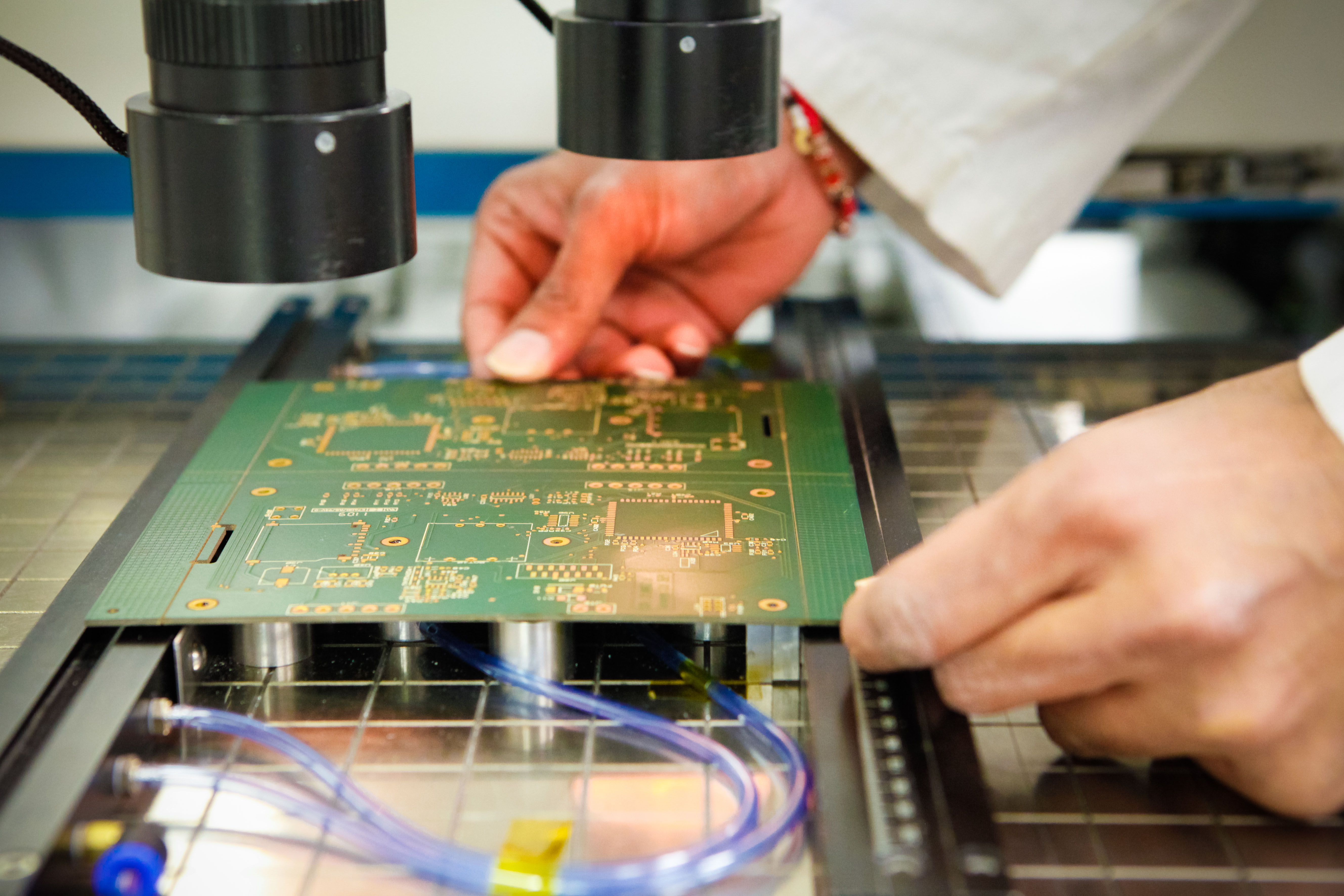
That involves carefully planning the placement of components and tracing the connection lines. In general, surface mount technology (SMT) has become more popular due to its ability to produce smaller and more complex PCBs with higher component densities, making them more suitable for modern electronics. However, through-hole components are still used for certain applications that require higher mechanical strength, higher current carrying capacity, or for components that need to be replaced easily. PCB manufacturing is a complex process that involves multiple steps and highly specialized equipment.
Place Components
These issues can cause malfunctions, reduced performance, and even complete failure of the electronic device. In some cases, poor EMC can also lead to regulatory compliance issues, as electronic products must meet specific EMC standards to be sold in certain markets. Typically, PCB design falls under the Hardware (HW) design category of engineering. It ties in electrical, mechanical, software, systems, test, and manufacturing disciplines to include electrical (ECAD) and mechanical (MCAD) designers.
Thermal Vias and Heat Sinks
PCB: Basics of Design Series - Electronic Design
PCB: Basics of Design Series.
Posted: Thu, 28 Sep 2023 07:00:00 GMT [source]
If you place your components haphazardly, don’t be surprised when you have a bunch of unsoldered connections on your PCB. We haven’t been able to cover some other essential aspects of PCB board design, such as drill holes. We know, therefore, that you likely have more questions about PCB layout guidelines.
Quality Control and Assembly
After the layer stack is created and any impedance profiles are determined, it's time to set up your circuit board design rules so that you can start placing and routing components. Though a deep program, Altium Designer’s user-experience is highly rewarding for new and experienced PCB board designer experiences alike. It offers a design environment built from the ground up for a streamlined custom circuit board design process within a single, unified printed circuit board layout environment. On the layout side of PCB design, the schematic connectivity is received and processed as nets that connect two or more component pins. With an outline of the intended board shape on the screen, the layout designer will place the component footprints in the correct locations. Once these components are optimally organized, the next step is to connect the nets to the pins by drawing the traces and planes between the pins.
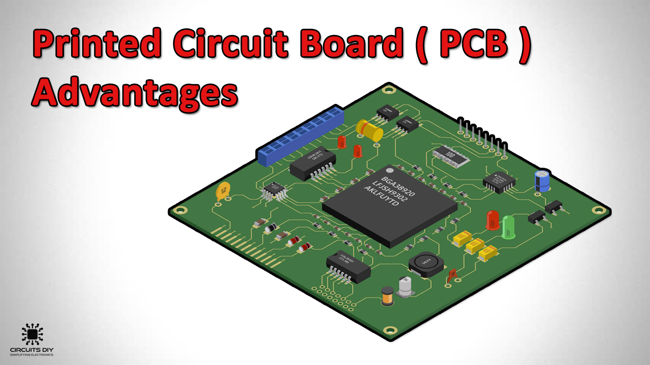
Common layer configurations include power and ground planes, signal layers, and dedicated layers for specific purposes like shielding or heat dissipation. The bare PCB is made up of land patterns for components to be attached/soldered on to the PCB. They are interconnected by a conductive printed wire referred to as a trace on a non-conductive substrate.
In this tutorial, we'll show all the steps involved in creating your circuits and schematics, then we'll transition into creating a circuit board design that can actually be manufactured. Printed circuit boards came from electrical connection systems that were used in the 1850s. Originally metal strips or rods were used to connect large electric components mounted on wooden bases.
The vast majority of PCBs have 1 ounce of copper per square foot but some PCBs that handle very high power may use 2 or 3 ounce copper. Each ounce per square translates to about 35 micrometers or 1.4 thousandths of an inch of thickness of copper. To design a Printed Circuit Board (PCB), you need to draw holes, pads, and wires for your circuit.
These rules can be applied to individual objects or to groups of objects using queries or using Net Class objects. Take a look at this article to see how you can set up a Net Class in Altium Designer. When you transfer your schematic information to the PcbDoc the component footprints are shown in addition the board outline specified. Prior to placing components you should define the PCB layout (i.e. shape, layer stackup) using the Layer Stackup Manager, shown below.
No comments:
Post a Comment